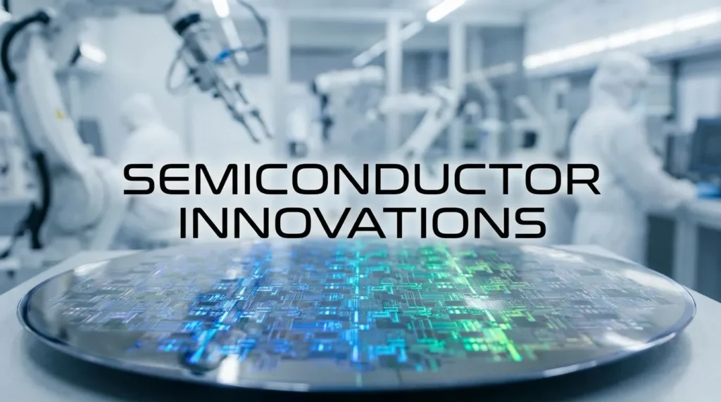
Let’s skip the standard timeline approach and drop right into the physical dirt of modern manufacturing. If you want to grasp the exact mechanics of how semiconductor innovation is changing the world, you have to stop looking at software and look at what happens when hardware stops scaling and starts stacking.
This year, the sheer physical absurdity of fitting well over 100 billion transistors onto a single piece of silicon actually became a mass-production reality.
We watched it happen in real-time with the aggressive rollout of 2nm-class nodes like TSMC’s N2 and Intel’s 18A. We are no longer just printing microscopic circuits for standard laptops. We are building invisible, hyper-dense cities on brittle wafers of sand, and the heat output is genuinely terrifying.
Why Semiconductor Innovation Now Means Vertical Stacking
Trying to cram every functional block onto a single monolithic die is essentially a dead practice. The defect rates get too high. The production costs spiral completely out of control.
Building a Monolithic processor in 2026 is like pouring a functioning latest city out of one single block of concrete.. instead of assembling it piece by piece.
Instead, the Industry relies densely on Chiplets & advanced Chip-on-Wafer-on-Substrate packaging. They manufacture different functional blocks in different facilities. And then they test them for flaws & painstakingly stitch together in high-density 3D packages.
You stack highly specialized prefabricated modules directly on top of each other. It bypasses the physical limits of extreme scaling simply by building upward.
Shrinking Nodes and Power Delivery Innovations
Companies are not just making transistors smaller anymore. The physics simply will not allow it without melting the silicon into expensive slag. Because traditional scaling hit a thermal wall, engineers entirely flipped the power delivery model.
Enter backside power delivery. This is the unglamorous but intensely effective structural hack where electricity gets routed entirely underneath the transistor layer to free up the front side for pure signal routing.
It fundamentally reorganizes the die. This specific structural change slashes power consumption across power-hungry global data centers, forces engineers to entirely unlearn decades of chip design, and physically separates power lines from the chaotic traffic jam of data signals.
No broad generalizations here. This is just the gritty reality of 1.8nm and 2nm architecture keeping modern server farms from catching fire.
Semiconductors Pushing World AI Out of the Cloud
Everyone assumes artificial intelligence lives entirely in massive server farms. They are wrong.
Right now, the hardware pyramid is collapsing. Semiconductor revenue is heavily shifting toward edge inference as of 2026. We are seeing domain-specific AI processors hardwired directly into daily devices.
They sit quietly in modern vehicles, mobile phones, and automated factory tools to immediately cut latency and violently slash server-side cloud computing costs.
The hardware innovation is no longer just about generating raw computing speed for big tech companies. It is about figuring out how to make a complex AI model run completely locally in your pocket without instantly draining the phone’s power cell or overheating the battery casing.
The Approaching Trillion Dollar Semiconductor Milestone
The global semiconductor market is officially projected to hit the staggering $975 billion mark this year. National security, massive corporate monopolies, and sensitive global supply chains now completely revolve around who exactly controls extreme-ultraviolet lithography machines and substrate packaging capacity.
Countries are effectively hoarding advanced silicon output the way they used to ruthlessly hoard crude oil reserves in the 1970s. We reached a bizarre point in human history where the entire global economic balance rests on microscopic wires.